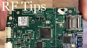
What are the challenges of integrating RF modules onto a PCB?
challenges of integrating RF modules onto a PCB
RF PCBs are designed to carry radio frequency (RF) signals in the range of 50 MHz to 1 GHz for AM/FM transmission and signals up to 2 GHz for microwave communication. These specialized circuit boards require a wide variety of features to optimize signal paths and reduce interference and noise. They also need to be able to resist the effects of vibration and environmental conditions. This is why choosing the right material for a rf pcb is so important.
The most important element of a RF circuit board is its substrate material. The selected material must support RF frequencies and have the appropriate dielectric constant, loss tangent, and coefficient of thermal expansion for seamless use. The material must also be moisture resistant to prevent damage from exposure to water or other chemicals.
Other design considerations include the ability to conduct high-speed signals, the presence of EMI/EMC considerations, and the ability to handle large amounts of power. High-speed signal propagation requires careful routing and space definition to avoid resonant traces that cause interference and reduce performance. RF circuits are particularly susceptible to the skin effect, which occurs when current only occupies the outer surface of a conductor and causes increased resistance. The placement of RF components must be carefully considered to minimize parasitic capacitance and inductance, which can lead to a variety of noise types including white, pink, or band limited noise as well as flicker, thermal, shot, phase, and avalanche noise.
What are the challenges of integrating RF modules onto a PCB?
In addition, RF circuits must be shielded from electromagnetic interference caused by internal circuits and other devices, as well as external sources such as magnetic fields. EMI/EMC mitigation is achieved through careful layer stack-up design, the use of ground planes, component placement, and impedance matching. The etching process must be tightly controlled to ensure that the widths and spacings of RF traces are accurate to the design specifications.
Pre-manufacturing testing is also essential for RF PCBs to ensure that the manufactured boards meet all the necessary tolerances. Testing techniques like time-domain reflectometry can help detect impedance mismatches, signal reflections, and other issues that can degrade the quality of an RF circuit board.
Using simulation software can help address these challenges by allowing designers to test and refine their designs before moving on to manufacturing. They can adjust trace widths and spacings, rework RF stack-ups, and move components around virtually to see how their changes affect impedance, noise, and signal flow before they commit them to the manufacturing process. This allows them to iteratively improve the design and avoid costly production mistakes. Ultimately, the right software will make it easy to create a professional-grade RF circuit board that delivers the performance required for your application. This will ensure that you can be confident your RF circuit board will meet the demands of any application, even in harsh environments.
Selecting the appropriate RF PCB (Printed Circuit Board) stackup configuration is crucial for achieving optimal performance in high-frequency electronic devices. The stackup configuration refers to the arrangement of layers within the PCB, including signal, ground, and power planes. Here’s a guide on how to choose the right RF PCB stackup configuration.
Leave a Reply